- 您现在的位置:买卖IC网 > Sheet目录2000 > IDTSSTE32882KA1AKG (IDT, Integrated Device Technology Inc)IC REGISTERING CLK DRIVER 176BGA
1.25V/1.35V/1.5V REGISTERING CLOCK DRIVER WITH PARITY TEST AND QUAD CHIP SELECT
18
SSTE32882KA1
7314/8
THE INFORMATION IN THIS DOCUMENT IS SUBJECT TO CHANGE WITHOUT NOTICE
SSTE32882KA1
1.25V/1.35V/1.5V REGISTERING CLOCK DRIVER WITH PARITY TEST AND QUAD CHIP SELECT
COMMERCIAL TEMPERATURE RANGE
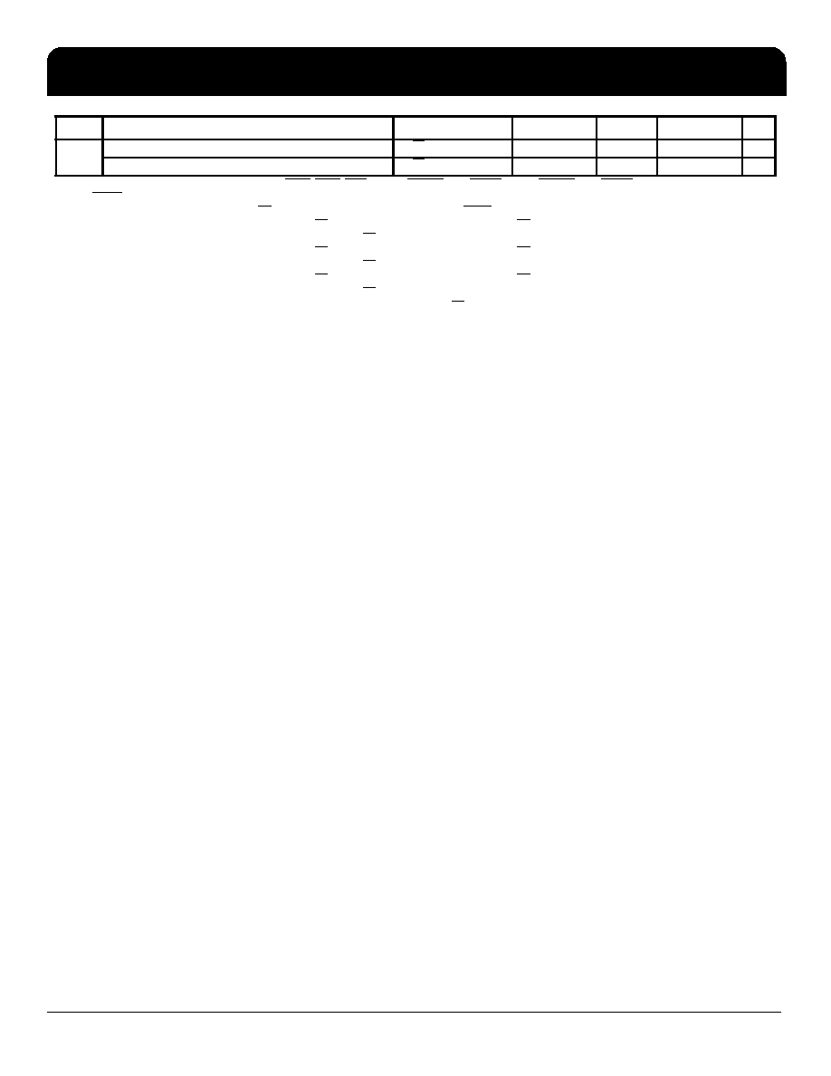
VOX
Differential Output Crosspoint Voltage (1.5V Operation)
Yn, Yn
0.5xVDD – 100 mV
–
0.5xVDD + 100 mV
V
Differential Output Crosspoint Voltage (1.35V Operation)
Yn, Yn
0.5xVDD – 90 mV
–
0.5xVDD + 90 mV
V
1 DCKE0/1, DODT0/1, DA0..DA15, DBA0..DBA2, DRAS, DCAS, DWE, PAR_IN, DCS[1:0] when QCSEN = HIGH, DCS[3:0] when QCSEN = LOW.
2 RESET, MIRROR
3 This spec applies only when both CK and CK are actively driven LOW. It does not apply when CK/CK are floating.
4 Extended range for Vix is only allowed for clock (CK and CK) and if single-ended clock input signals CK and CK are monotonic with a single-ended swing VSEL / VSEH
of at least VDD/2 +/-275 mV, and when the differential slew rate of CK - CK is larger than 4 V/ns.
5 Extended range for Vix is only allowed for clock (CK and CK) and if single-ended clock input signals CK and CK are monotonic with a single-ended swing VSEL / VSEH
of at least VDD/2 +/-243 mV, and when the differential slew rate of CK - CK is larger than 4 V/ns.
6 Extended range for Vix is only allowed for clock (CK and CK) and if single-ended clock input signals CK and CK are monotonic with a single-ended swing VSEL / VSEH
of at least VDD/2 +/-243 mV, and when the differential slew rate of CK - CK is larger than 3.6 V/ns
7 VID is the magnitude of the difference between the input level on CK and the input level on CK See Diagram (Voltage waveforms; input clock)
8 Default settings
Symbol
Parameter
Signals
Min
Nom
Max
Unit
发布紧急采购,3分钟左右您将得到回复。
相关PDF资料
ISD1750SYR
IC VOICE REC/PLAY 50SEC 28-SOIC
ISD5008EYI
IC VOICE REC/PLAY 4-8MIN 28-TSOP
ISL12008IB8Z
IC RTC I2C LO-POWER 8-SOIC
ISL12020MIRZ-T7A
IC RTC/CALENDAR TEMP SNSR 20DFN
ISL12022IBZ-T7A
IC RTC/CALENDAR TEMP SNSR 8SOIC
ISL12022MAIBZ
IC RTC/CALENDAR TEMP SNSR 20SOIC
ISL12022MIBZ-T7A
IC RTC/CALENDAR TEMP SNSR 20SOIC
ISL12022MIBZR5421
IC RTC/CALENDAR TEMP SNSR 20SOIC
相关代理商/技术参数
IDTSSTE32882KA1AKG8
制造商:Integrated Device Technology Inc 功能描述:IC REGISTERING CLK DRIVER 176BGA
IDTSSTUB32866BHLF
功能描述:IC BUFFER 25BIT CONF REG 96LFBGA RoHS:是 类别:集成电路 (IC) >> 接口 - 专用 系列:- 特色产品:NXP - I2C Interface 标准包装:1 系列:- 应用:2 通道 I²C 多路复用器 接口:I²C,SM 总线 电源电压:2.3 V ~ 5.5 V 封装/外壳:16-TSSOP(0.173",4.40mm 宽) 供应商设备封装:16-TSSOP 包装:剪切带 (CT) 安装类型:表面贴装 产品目录页面:825 (CN2011-ZH PDF) 其它名称:568-1854-1
IDTSSTUB32S869AHLF
功能描述:IC REGISTERED BUFFER 150-TFBGA RoHS:是 类别:集成电路 (IC) >> 接口 - 信号缓冲器,中继器,分配器 系列:- 标准包装:160 系列:- 类型:转发器 Tx/Rx类型:以太网 延迟时间:- 电容 - 输入:- 电源电压:2.37 V ~ 2.63 V 电流 - 电源:60mA 安装类型:表面贴装 封装/外壳:64-TQFP 裸露焊盘 供应商设备封装:64-TQFP-EP(10x10) 包装:托盘 其它名称:Q5134101
IDTSSTUB32S869AHLFT
功能描述:IC REGISTERED BUFFER 150-TFBGA RoHS:是 类别:集成电路 (IC) >> 接口 - 信号缓冲器,中继器,分配器 系列:- 标准包装:160 系列:- 类型:转发器 Tx/Rx类型:以太网 延迟时间:- 电容 - 输入:- 电源电压:2.37 V ~ 2.63 V 电流 - 电源:60mA 安装类型:表面贴装 封装/外壳:64-TQFP 裸露焊盘 供应商设备封装:64-TQFP-EP(10x10) 包装:托盘 其它名称:Q5134101
IDTSSTVF16857AGLF
功能描述:IC DDR REGISTER 48-TSSOP RoHS:是 类别:集成电路 (IC) >> 接口 - 专用 系列:- 标准包装:3,000 系列:- 应用:PDA,便携式音频/视频,智能电话 接口:I²C,2 线串口 电源电压:1.65 V ~ 3.6 V 封装/外壳:24-WQFN 裸露焊盘 供应商设备封装:24-QFN 裸露焊盘(4x4) 包装:带卷 (TR) 安装类型:表面贴装 产品目录页面:1015 (CN2011-ZH PDF) 其它名称:296-25223-2
IDTSTAC9200X3NAEB1X
功能描述:IC AUDIO CODEC 2CH HD 32-QFN RoHS:是 类别:集成电路 (IC) >> 接口 - 编解码器 系列:- 标准包装:2,500 系列:- 类型:立体声音频 数据接口:串行 分辨率(位):18 b ADC / DAC 数量:2 / 2 三角积分调变:是 S/N 比,标准 ADC / DAC (db):81.5 / 88 动态范围,标准 ADC / DAC (db):82 / 87.5 电压 - 电源,模拟:2.6 V ~ 3.3 V 电压 - 电源,数字:1.7 V ~ 3.3 V 工作温度:-40°C ~ 85°C 安装类型:表面贴装 封装/外壳:48-WFQFN 裸露焊盘 供应商设备封装:48-TQFN-EP(7x7) 包装:带卷 (TR)
IDTSTAC9200X3NAEB1XR
功能描述:IC AUDIO CODEC 2CH HD 32-QFN RoHS:是 类别:集成电路 (IC) >> 接口 - 编解码器 系列:- 标准包装:2,500 系列:- 类型:立体声音频 数据接口:串行 分辨率(位):18 b ADC / DAC 数量:2 / 2 三角积分调变:是 S/N 比,标准 ADC / DAC (db):81.5 / 88 动态范围,标准 ADC / DAC (db):82 / 87.5 电压 - 电源,模拟:2.6 V ~ 3.3 V 电压 - 电源,数字:1.7 V ~ 3.3 V 工作温度:-40°C ~ 85°C 安装类型:表面贴装 封装/外壳:48-WFQFN 裸露焊盘 供应商设备封装:48-TQFN-EP(7x7) 包装:带卷 (TR)
IDTSTAC9200X3TAEB1X
功能描述:IC AUDIO CODEC 2CH HD 48-LQFP RoHS:是 类别:集成电路 (IC) >> 接口 - 编解码器 系列:- 标准包装:2,500 系列:- 类型:立体声音频 数据接口:串行 分辨率(位):18 b ADC / DAC 数量:2 / 2 三角积分调变:是 S/N 比,标准 ADC / DAC (db):81.5 / 88 动态范围,标准 ADC / DAC (db):82 / 87.5 电压 - 电源,模拟:2.6 V ~ 3.3 V 电压 - 电源,数字:1.7 V ~ 3.3 V 工作温度:-40°C ~ 85°C 安装类型:表面贴装 封装/外壳:48-WFQFN 裸露焊盘 供应商设备封装:48-TQFN-EP(7x7) 包装:带卷 (TR)